Technology · NEWS EXPLAINER
Samsung will use TSMC’s 3nm process for Nvidia NVHBM base dies, report says
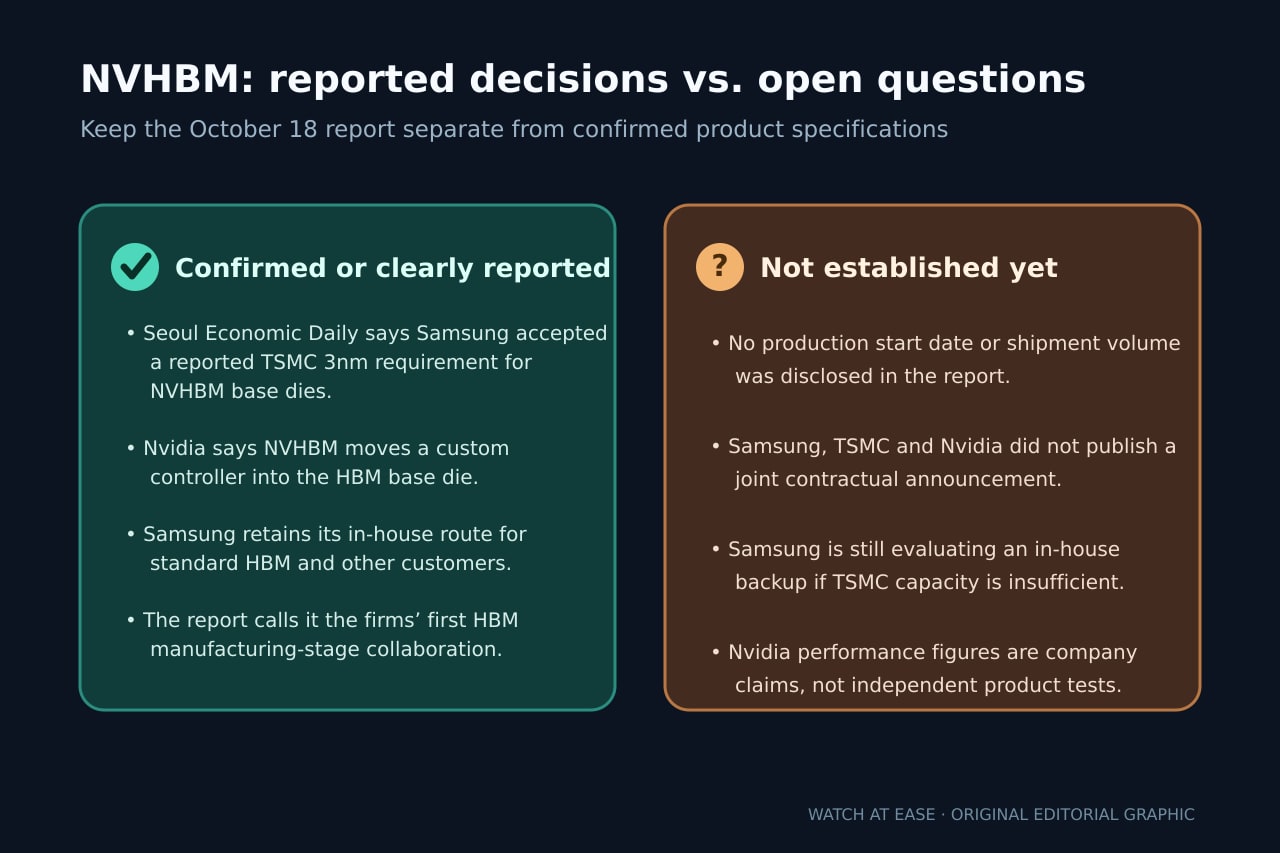
Seoul Economic Daily says Samsung accepted Nvidia’s common base-die requirement for custom HBM. Nvidia confirms the architecture; production dates, volumes and contract terms remain undisclosed.
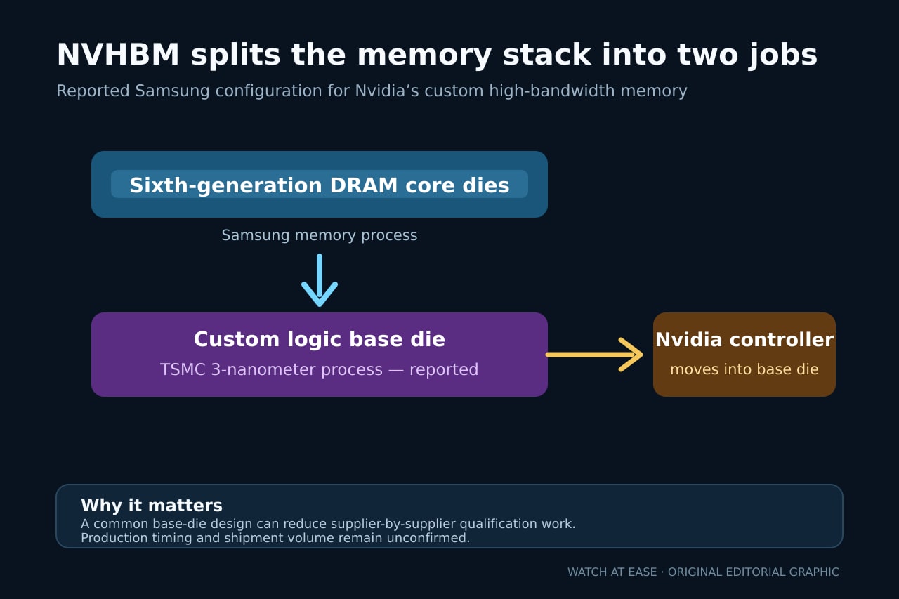
Samsung Electronics will use TSMC’s 3-nanometer process for the custom logic base die in Nvidia’s NVHBM, Seoul Economic Daily reported on October 18. The report says Samsung would keep making the stacked DRAM core dies. Nvidia confirms that NVHBM moves its custom controller into the base die, but none of the three companies has jointly announced the reported foundry arrangement.
What the October 18 report says
Seoul Economic Daily says Samsung accepted Nvidia’s requirement to use TSMC’s 3nm process for the NVHBM base die while supplying sixth-generation 1c DRAM for the stacked core dies. The newspaper calls this Samsung and TSMC’s first cooperation at the HBM manufacturing stage. Reuters repeated the report but cited the Seoul newspaper, so those two accounts are one reporting origin rather than two independent confirmations.
Why the base die matters in NVHBM
Nvidia’s official explanation says NVHBM places a custom memory controller in the logic base die under the memory stack. Nvidia says that design can deliver up to 30% more bandwidth, 15% lower HBM power and 25% more area for accelerators. Those numbers are company claims for the architecture, not independent product tests or confirmed Samsung shipment specifications.
A common design changes qualification, not who makes the memory
Nvidia says its base-die implementation is standardized across multiple memory providers. A common design can reduce supplier-specific qualification work for the controller layer, but it does not mean TSMC would make Samsung’s DRAM core dies. Under the reported configuration, Samsung remains the memory supplier and TSMC fabricates the custom logic base die.
Samsung’s in-house route is not disappearing
The October 18 report says Samsung would continue using its own foundry for standard HBM and for custom HBM sold to other customers. TrendForce had independently described a dual-track strategy on October 9: Samsung could pair its own core dies with either Samsung Foundry or TSMC base dies depending on customer requirements. The new report narrows that broader strategy to Nvidia’s requested configuration.
What remains unconfirmed before production
Samsung, TSMC and Nvidia have not issued a joint contractual announcement with a production start, shipment volume, pricing or contract value. Seoul Economic Daily also says Samsung is evaluating an in-house fallback if TSMC capacity is insufficient. Until a company filing, product specification or production notice appears, the careful conclusion is a reported sourcing decision supported by known NVHBM architecture—not a confirmed shipping schedule.